
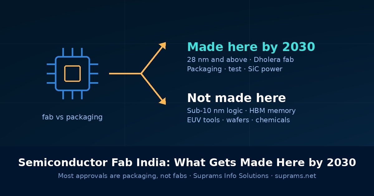
A semiconductor fab in India is not the same thing as a chip packaging plant, and most of what has been approved under the India Semiconductor Mission is the latter. As of September 2026 the country has several assembly and test facilities in various stages of construction and commissioning, one large commercial wafer fabrication plant under construction in Gujarat, a compound semiconductor fab approved in Odisha, and a small government-owned legacy fab in Punjab. What that adds up to by 2030 is real capacity in mature-node and packaged chips, not leading-edge processors.
Fabrication, assembly and test are not the same thing
The confusion in most coverage comes from treating one long manufacturing chain as a single word.
- Wafer fabrication is the front end. Silicon wafers go through lithography, etch and deposition to create transistors. This is what people mean by a fab, and it needs extreme cleanroom standards, ultrapure water at very large volumes and tools costing tens of millions of dollars each.
- Assembly, test, mark and pack, usually shortened to ATMP or sold as OSAT, is the back end. Finished wafers are cut into dies, bonded, encased, tested and marked. It is capital-intensive but an order of magnitude less so than a fab, and it employs more people per rupee invested.
- Design produces the circuit itself and needs almost no factory at all.
A plant that only does ATMP does not make chips in the sense most readers assume. It finishes them. That is genuinely valuable work and it is where India's manufacturing entry sensibly begins, but calling it a fab sets expectations that will not be met.
What has been approved, and what kind of plant each is
The India Semiconductor Mission sits under the Ministry of Electronics and Information Technology and was approved in December 2021 with an outlay of ₹76,000 crore. The projects cleared since then, with their announced investment figures, break down roughly as follows.
Wafer fabrication
- Dholera, Gujarat — a joint venture between an Indian conglomerate's electronics arm and a Taiwanese foundry partner, approved in February 2024 at an announced ₹91,000 crore. This is India's first commercial wafer fab and is aimed at mature nodes, publicly described as 28 nanometre and above.
- Odisha — a silicon carbide compound semiconductor fab approved in 2025. Compound semiconductors serve power electronics and electric vehicles rather than computing.
- Mohali, Punjab — the existing government Semi-Conductor Laboratory, a legacy facility at 180 nanometre used largely for strategic and space applications, with modernisation proposals discussed for several years.
Assembly, test and packaging
- Sanand, Gujarat — a large ATMP plant from a US memory manufacturer, approved in June 2023, packaging and testing DRAM and NAND
- Jagiroad, Assam — an assembly and test plant announced at around ₹27,000 crore
- Sanand, Gujarat — an OSAT joint venture involving an Indian power electronics group with Japanese and Thai partners
- Sanand, Gujarat — a further OSAT approved in September 2024
- Jewar, Uttar Pradesh — a display driver chip packaging joint venture approved in May 2025
Announced timelines for several of these have moved at least once, and investment figures quoted publicly are project totals across multiple phases rather than money already spent. The current status of each project is published by the India Semiconductor Mission, and that is the source to check before repeating any date, including the ones in this article.
Nodes: why 28 nanometre and above is the sensible target
Leading-edge logic in 2026 means 3 nanometre and below, produced by a very small number of companies using extreme ultraviolet lithography tools. A single such tool costs upwards of US$150 million, supply is allocated years in advance, and a leading-edge fab runs into tens of billions of dollars before it makes anything.
Mature nodes, broadly 28 nanometre and larger, are a different business. The equipment market is deeper, second-hand tools exist, the process is well understood and yield ramps faster. The demand is also enormous and unglamorous.
- Automotive electronics, where a single vehicle contains hundreds of chips, most of them on old nodes
- Power management, motor control and industrial sensing
- Consumer appliances, lighting, metering and set-top boxes
- Microcontrollers for everything from fans to feature phones
Those are the chips India plausibly makes domestically by 2030. They are also the chips whose shortage stopped car production lines worldwide during the pandemic supply crunch, so mature-node capacity is a strategic asset even though it never appears in a phone launch.
What India will not be making by 2030
Realistic expectations matter more than enthusiasm here.
- Leading-edge logic. No announced project targets sub-10 nanometre production, and none plausibly could inside this decade.
- High-bandwidth memory for AI accelerators. The memory investment announced so far is packaging and test, not memory fabrication.
- Advanced lithography equipment. The tool supply chain is concentrated in Europe, Japan and the United States and is not being replicated.
- Full supply-chain independence. Wafers, gases, photoresists and specialty chemicals are largely imported, and a fab without that ecosystem nearby carries a cost penalty.
None of that makes the programme a failure. It means the honest description is import substitution and supply-chain resilience at mature nodes, with packaging as the near-term win.
The design side was always the strength
India has had large semiconductor design operations for decades. A substantial share of the world's chip design and verification engineering already happens in Bengaluru, Hyderabad, Pune and Noida for global firms, and the Design Linked Incentive scheme has supported domestic fabless startups.
The interesting question for the next five years is whether domestic design work starts taping out at domestic fabs. A local mature-node foundry plus a local OSAT plus local design is a complete loop for industrial and automotive parts, and that loop is what would actually change the economics.
What this means if you buy IT hardware in India
Honest answer: not much before 2030, and nothing at all for laptops and servers. Domestic mature-node output does not change what a business pays for a Windows server or a switch, because those parts come from leading-edge and advanced packaging supply chains that remain offshore.
Where it may show up sooner is in lead times and pricing for industrial equipment, power electronics, metering and automotive components, and in a somewhat shorter supply chain during a global shortage. For procurement planning, keep treating hardware lead times as a global variable rather than a local one, and keep the refresh and support terms tight, as set out in the IT AMC contract checklist for Delhi NCR.
The bigger near-term operational story for most businesses is still software, not silicon. What changes a mid-sized company's cost base this year is the kind of automation described in the piece on AI agents Indian SMBs are running in 2026.
How to check the current position
This topic moves. Project timelines slip, phases get re-announced, and press coverage frequently describes packaging plants as fabs.
- Treat the India Semiconductor Mission and MeitY pages as the primary source for approvals and status
- Read announced investment as a multi-phase total, not as capital deployed
- Check whether a named facility does fabrication or assembly and test before drawing conclusions
- Note the node. A 28 nanometre fab and a 3 nanometre fab are different industries, not different sizes of the same thing
What to do next
If semiconductors touch your procurement, build a habit of verifying plant type and node before acting on a headline. If they do not, the practical takeaway is narrower: domestic capacity will improve resilience for industrial and automotive parts over this decade and will not change your server refresh cycle.
More analysis of this kind is published on the Suprams technology blog. For questions about hardware procurement or IT planning, call +91-859-517-4178 or write to info@suprams.net during office hours, Monday to Friday 10:00 to 19:00 IST.